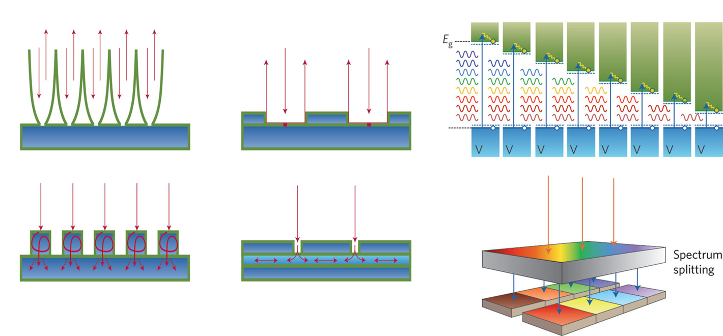
Microphotonic & Nanophotonic Structures (left) and Optically Parallel Multijunctions (right)
A. Polman & H.A. Atwater Nature Materials 11, 174–177 (2012)
Full Spectrum Ultrahigh Efficiency
The Full Spectrum Photovoltaics team is designing and building a spectrum-splitting photovoltaic module that will achieve unprecedentedly high efficiency. Single-junction solar cells are most efficient for a narrow band of light. Lack of absorption of low energy photons and thermalization of high-energy photons leads lead to a loss of over 40% of incident solar power. Current-matching and lattice-matching restrictions limit the efficiency of traditional monolithic multijunction solar cells. The most efficient modules today convert 36% of incident power. In order to avoid these limitations and realize ultrahigh efficiency (close to 50%), we use optics to split sunlight into many color bands that get targeted at solar cells can most efficiently convert that band.
We have explored a series of device architectures and zeroed in on one to fabricate and test. This design incorporates six cells with bandgaps spanning the solar spectrum. Additionally, we use dichroic filters and compound parabolic concentrators for high concentration. During this process we learned that independent electrical connections to each cell increases both peak efficiency and overall annual energy production relative to series connected architectures. This is done by reducing performance drop-offs when the spectrum shifts from its noontime peak giving up to a 20% boost in annual energy production.
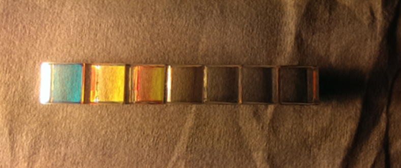
Spectrum Splitting PV Module
Beyond demonstrating that ultrahigh efficiency is possible, we aim to decrease the levelized cost of electricity (LCOE = {total lifetime cost} ÷ {total lifetime energy production}). By increasing efficiency and annual energy production, we push total energy production up, thereby reducing an important cost metric. We also use on-going cost-modeling to ensure that our designs are practical and on track for low LCOE. This includes exploring high-constrast gratings, polymer based dichroics and alternate filter materials as well as alternative building integrated designs.
Earth Abundant PV Materials
The Earth Abundant PV team is investigating several alternative materials that can potentially replace or complement traditional silicon photovoltaics. Materials being studied include well known alternatives such as Cu2O and Zn3P2, as well as new materials such as ZnSnN2 and its quaternary alloys.
Cu2O
Cu2O is an earth abundant semiconductor that has been identified as a promising photovoltaic material due to its high absorption and good minority carrier diffusion length. Cu2O is intrinsically p-type and thus requires a heterojunction partner to enable charge separation, which introduces the possibility of increased interface defects. The highest reported photovoltaic efficiency for a Cu2O absorber device is approximately 5%, whereas the detailed balance limit has been calculated to exceed 20%. One of the main reasons for low efficiency is instability of the Cu2O surface with respect to oxidation or reduction. We have produced high quality Cu2O both in bulk form by thermal oxidation as well as by plasma-assisted molecular beam epitaxy (MBE). Goals of the project include elucidating how device performance is affected by surface structure and composition, band alignments, defects, and new heterojunction partners.
Zn3P2
The prospect of terawatt-scale electricity generation using a photovoltaic (PV) device places strict requirements on the active semiconductor’s optoelectronic properties and elemental abundance. After reviewing the constraints placed on an “earth-abundant” solar absorber, we find zinc phosphide (α-Zn3P2) to be an ideal candidate. In addition to its near-optimal direct band gap of 1.5 eV, high visible-light absorption coefficient (>104 cm-1), and long minority-carrier diffusion length (>5 µm), Zn3P2 is composed of abundant Zn and P elements and has excellent physical properties for scalable thin-film deposition. However, to date a Zn3P2 device of sufficient efficiency for commercial applications has not been demonstrated. Record efficiencies of 6.0% for multicrystalline and 4.3% for thin-film cells have been reported, respectively. Performance has been limited by Zn3P2’s intrinsic p-type conductivity which restricts us to Schottky and heterojunction device designs. Due to our poor understanding of Zn3P2 interfaces, an ideal heterojunction partner has not yet been found.
The goal of our work is to explore the upper limit of solar conversion efficiency achievable with a Zn3P2 absorber through the design of an optimal heterojunction PV device. To do so, we investigate three key aspects of material growth, interface energetics, and device design. First, the growth of Zn3P2 on GaAs(001) is studied using compound-source molecular-beam epitaxy (MBE). We successfully demonstrate the pseudomorphic growth of Zn3P2 epilayers of controlled orientation and optoelectronic properties. Next, the energy-band alignments of epitaxial Zn3P2 and II-VI and III-V semiconductor interfaces are measured via high-resolution x-ray photoelectron spectroscopy in order to determine the most appropriate heterojunction partner. From this work, we identify ZnSe as a nearly ideal n-type emitter for a Zn3P2 PV device. Finally, various II-VI/ Zn3P2 heterojunction solar cells designs are fabricated, including substrate and superstrate architectures, and evaluated based on their solar conversion efficiency.
Light Trapping and Collimation
TBD
III-V Materials and Devices
Unlike Si, many III-V semiconductors have direct electronic bandgaps well suited for applications involving light emission and absorption. Also, by alloying different materials during epitaxy, the bandgaps of III-V semiconductors can be tuned to span the entire visible region and into the infrared. As solar cells, III-V materials can absorb light very efficiently and can thus be made much thinner than solar cells made with indirect bandgap materials like Si. As a result, world record photovoltaic conversion efficiencies for both single and multi-junction solar cells have been achieved using III-V semiconductors. Additionally, due to their superior light emission properties, III-V materials are commonly used in light emitting diodes (LEDs) and lasers.
The Atwater group prepares thin-film III-V solar cells by epitaxial lift-off (ELO), a process in which a thin device is removed from its growth substrate and integrated with an arbitrary back reflector. III-V solar cells made in this way can have higher efficiencies than those kept on a growth substrate, as they have traditionally been made. After ELO, the cells can be modified with the broad portfolio of light trapping schemes studied by the Atwater group.
Similar to ELO, thin films of strained III-V materials can be exfoliated from their growth substrates and relaxed to form new “virtual” substrates with non-traditional lattice constants for further epitaxial growth. The Atwater group also takes advantage of the high efficiency of III-V solar cells in the Full Spectrum Ultrahigh Efficiency project, aimed at reaching over 50% conversion efficiency with the aid of spectrum splitting and optical concentration. III-V materials are also being explored in the Atwater group in microwire optoelectronics and solar fuel applications.
Silicon and Microwire Photovoltaics
TBD