Graphene Plasmonics
Graphene has attracted a lot of attention in recent years owing to the new physics that emerge when this single layer of carbon atoms can be isolated. Its unique band structure, high electronic mobility, and ultra-thin dimensionality make it a unique material for exploring strong light-matter interactions.
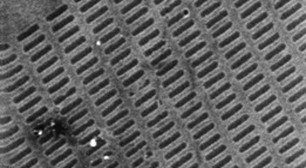
Our group is exploring graphene’s unique materials properties in the context of tunable plasmonics. By patterning Fabry-Perot nanoresonators into a doped graphene sheet we can measure a plasmonic resonance that varies with the width of the resonator. In addition, by controlling the charge carrier density in the graphene, achieved easily by applying a gate voltage across the material, we tune the spectral position and strength of the plasmonic resonance of the nanoresonators. These structures have an extremely small mode-volume, resulting in extremely strong interactions between the resonators and their environment.
We see this strong interaction manifested as composite modes formed between the graphene plasmon and phonons in the substrate it sits upon, including just a single layer of hexagonal boron nitride. We have farther explored the potential for these strong interactions by creating a graphene “Salisbury screen” in which we construct a unique geometry to maximize the light absorption into the resonators, achieving 24.5% absorption in a single layer of atoms. By doing this, we can control the interaction of graphene plasmons with a significant fraction of incident light.
Two-Dimensional Materials
Two-dimensional materials have attracted a great deal of attention within the scientific community over the past decade owing to the unique new physics that emerges as we transition from bulk to monolayer materials. Graphene, a single atomic layer of carbon atoms, in particular has optoelectronic properties distinct from those of any other known material – its linear bandstructure and monolayer thickness give it an extraordinarily high optical absorption per layer, as well as a high mobility that opens up the potential for very low loss processes, along with many other exotic properties. Being only a monolayer thick also allows for new techniques in enhanced light-matter interactions, one example being in tunable plasmonics.
The field of plasmonics explores the strong confinement of light in materials that results when incident radiation excites electrons to oscillate collectively. In graphene, this confinement is extremely strong due to the fact that it is less than 1nm thick. Because the fields near the graphene are extremely strong, it interacts very strongly with its surroundings, with the ability to couple with materials down to a single monolayer, for example hBN. By patterning graphene into small ribbons, it can couple efficiently to free-space, allowing the excitation of plasmons. By then changing the width of these ribbons, the resonant wavelength excited is shifted. In addition, because graphene is only one monolayer thick, its charge carrier density can be easily tuned by using an electrostatic gate – this also allows for actively tunable plasmonics. These plasmons, which absorb incident light, can also be exploited in a reciprocal process. By heating up graphene resonators, the plasmon becomes a tunable emitter of thermal radiation. The plasmonic nature of the graphene allows for ultrafast control of this radiation.
In addition to graphene, there exist other monolayer materials which are distinct because instead of being a semimetal, they are semiconductors. Transition metal dichalcogenides, such as MoS2 and MoSe2, are direct bandgap semiconductors, making them excellent candidates for ultrathin, lightweight solar cells. New light-trapping techniques can be used to enhance the absorption into these materials because of their two-dimensionality, leading to the potential for high-efficiency, low cost solar cells.

