V.E. Ferry, et.al., Applied Physics Letters 95 Art. #183503 (2009).
Tunable Plasmonic Materials
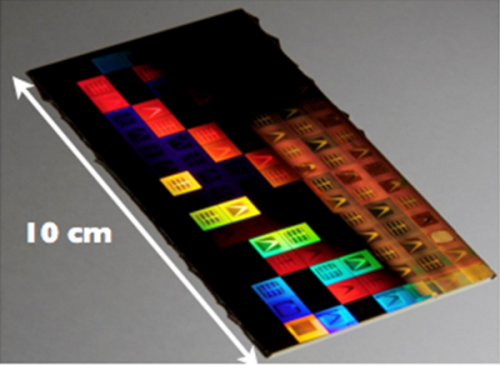
TBD
Plasmonic Devices and Circuits
Down-scaling optics to sub-wavelength dimension is one of the key challenges for developing optical nanocircuits and nanodevices. Plasmonics, the sub-wavelength surface electromagnetic waves that are guided on a metal-dielectric interface, enable a promising approach for achieving such down-scaling due to its extreme light confinement. Our group studies the physics and material sciences of plasmonic devices and develops several important components for the realization of future photonic/plasmonic integrated nanocircuit. We fabricate different plasmonic devices using nanofabrication techniques, such as ebeam lithography, focused ion beam lithography (FIB), and characterize the propagating plasmonic properties by Near Field Scanning Optical Microscopy (NSOM) and cross-polarization far-field optical microscopy.
We develop a Yagi-style optical antennas for efficient light coupling from free space into the plasmonic slot waveguide at telecommunication wavelength (45% in coupling, 60% total emission) (Fig. 1). Using this platform, we also experimentally demonstrate optical directional couplers (ODC) with extraordinarily short coupling length (top, right). Such plasmonic ODC out perform the Si-integrated circuitry components in terms of coupling-length-overloss ratio.
Active control of light at the nanoscale with plasmonic waveguides is one of the keys for future photonic/plasmonic chip integration where the plasmonic signals need to be modulated for data processing. We demonstrate an ultra-compact plasmonic slot waveguide field-effect modulator based on a transparent conducting oxide (TCO) active region (Fig.1, bottom). An important property of TCOs is that their carrier concentration can be significantly altered via application of electrical bias, similar to the field-effect MOS-devices where an accumulation layer is formed via field-effect dynamics, subsequently inducing a change in the local index of refraction. We integrate the TCO material into highly confined plasmonic slot waveguides to produce modulators with high dynamic range (3.2 dB/μm) and low waveguide loss (~ 0.45 dB/μm) via field-effect dynamics. Our team also investigates several mechanisms to further enhance the modulated on-off ratio, for instance resonant-interference based and epsilon-near-zero based enhancement, providing insight towards development of ideal plasmonic modulator/switch for future communication system.
Our group proposed that resonant guided wave networks (RGWNs) can engineer dispersion through wave resonances in a waveguide network consisting of waveguides coupled at their intersections. Using silicon waveguide coupled plasmonic structures, we experimentally demonstrate the concept of RGWN by showing a 90-degree CPP waveguide crossing operates as an ultra-compact equal-power-splitting element for sub-wavelength plasmonic nano-circuit elements (Fig. 2, left). Combining two basic plasmonic network elements, waveguides and splitters, we demonstrate a prototype plasmonic nanocircuit composed of four v-groove waveguides in an evenly spaced 2×2 configuration, which functions as a compact optical logic device at telecommunication wavelengths, routing different wavelengths via different on/off combinations to separated transmission ports (Fig.2 , right).
Plasmonic Solar Cells
TBD